Is customization in PCB assembly service have become a new approach to get state-of-the-art electronic design and manufacturing solutions?


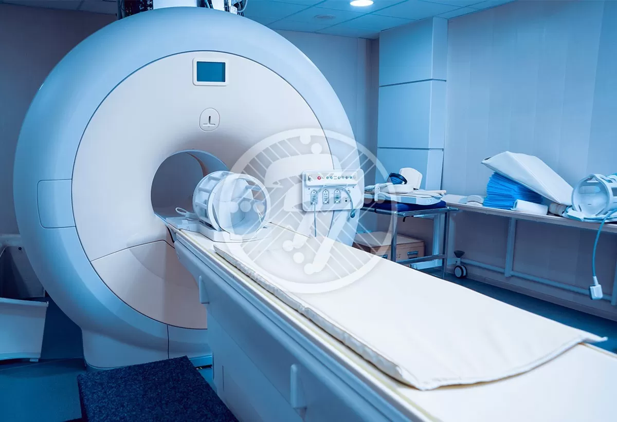
With the multiplying discovery and innovation of newer concepts and features, customization has been adopted into the products and processes of all the dominant markets. There has been a fostering notion of customization from computers, automobile, aircraft, robotics, telecommunication, pharmaceutics, defense, wagon wheel to the electronic household appliances.
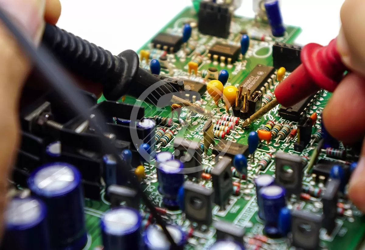
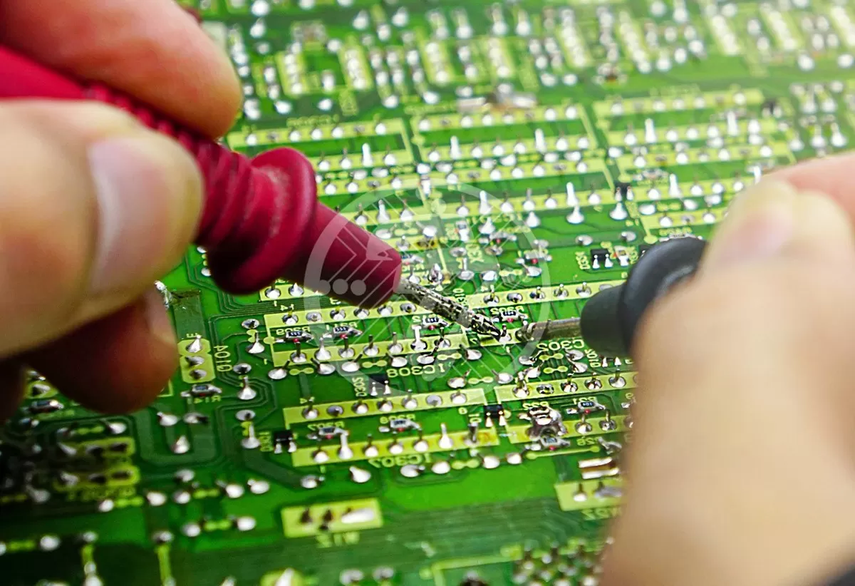
The different versions of modeling, remodeling, upgrading, reworking, altering and controlling assists in providing a prominent edge to affix and fit the exact needs of the customers. A complete spectrum of customized methodologies has high applicability in electronics world. TechnoTronix, one of the leading providers of electronic solutions with high end customization in PCB fabrication and PCB Prototyping requirements of its clients from varied industries, has a standardized process for developing a custom functional design as per the project specification. Check out the Top Manufacturing Factors That Affect the Cost of Custom PCB Board Assembly.
There has been a contradiction between manufacturing high volume with many novelties or prototyping highly customized PCB in low volumes. The dynamicity in the outlook as well as the nature of the PCB depends on the space occupancy, the spare parts and the accessories to be mechanized into the PCB.
TechnoTronix adopts customization in its offerings as well as in the PCB Assembly process to deliver a holistic solution in the prototype with state-of-art layouts it fabricates. From small updates to new product launch, it has a unique way to use advanced techniques with compact custom tools for mass customization and prototyping demands.
Thus, with an unfolding advancement in researches, numerous PCB Layout and prototypes with state-of-art techniques is in great fashion with the hike in demand every other day. To take a look at highly customized PCB assembly services,
At Technotronix, we combine state-of-the-art technology with our advanced engineering to deliver unparalleled quality and service. With fast PCB prototyping and consistent delivery of high-quality PCBs, we offer a robust source of competitive advantage to our clients. With our four decades of experience, you can rest assured that we are cognizant of the industry best practices and will keep you ahead of the curve. Visit to know more about PCB prototyping service and feel free to contact us. Also, you can drop an email to us at sales@technotronix.us.