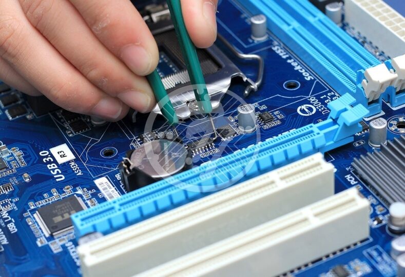
The Fortunes Of Using Heavy Copper In PCB Fabrication

The PCB fabrication is now a kernel of technological trends in current times across the globe. With rigorous development in technologies, the electronic instrument and components are also showing a pace in innovation every other day as the global market trends have turned into a dynamic one with ever changing customer preferences and demand for unique electronic products. This is where the electronic manufacturer and PCB fabricator have the same concern for reliable, high quality, cost effective electronic solution even in case of complex critical pcb layout requirements. One of the recent growing trend in PCB fabrication is the utilization of heavy copper in PCB manufacturing. This article brings to light the enrichments of using heavy copper in printed circuit board fabrication. In addition to this, it also furnishes with the technical details on the construction of PCB’s with using of heavy copper substrate.
To suffice the increasing demand and preferences of customers from varied market, the trend of using heavy copper in PCB’s is becoming a “good show” to trap the present world of technology implementation. When we speak about printed circuit boards, they have their application in each and every aspect of human life. Right from telecommunication, medical, automotive, defense, aerospace, military to renewable energy, transportation, industrial sector and many other dominant industries. On the other hand, the demand for high tech electronic machinery and appliances that run faster, are compact, secured product to use and more efficient with high power performance is what the customers desire that keeps on moving ahead with introduction to new technology every other day. This has made the PCB industry to be on top of the heap when it comes to innovation and transformations. Be it a heat dispersion, fast speed, high frequency or other critical design requirements, heavy copper in PCB fabrication has proven high performance output. Check out the complete guide on Copper Balance in Printed circuit Board Fabrication.
When learning to cook a dish, we first tumble on the ingredients and recipe and then start cooking, the same way, lets get a clear picture on technical aspects of Heavy copper used in PCB manufacturing before taking a dive into understanding the core merits of the Heavy copper PCB.
The printed circuit boards manufactured with the use of heavy copper is constructed with a fine combination of copper plating and copper etching processes. As the thin sheets of copper foil, the layers are created with circuits. Further, the copper etching technique makes it possible to eliminate the unwanted copper and copper plating technology optimizes the copper thickness to Traces, Pads, Planes and Drilled holes on the circuit board. Final lamination of layers in circuit board is done using epoxy based substrate. These heavy copper PCB is made of thermo layers which is best suited in multilayer PCB construction. In short, the heavy copper PCB is fabricated with high usage of finished copper in the internal and external base of the circuit board that is also known as laminated deposition.
The fortunes of using heavy copper in PCB fabrication
- Best for a compact electronic solution as it utilizes less space with either removing or allocating minimum space for cooling fans or heat sinks.
- High current carrying capacity.
- Resistance to high temperature.
- High durable performance with use of heavy copper substrate.
- Easy transfer of heat to external heat sinks.
- High caliber to withstand repeated thermal cycling that is capable to destroy a normal PCB in flip of seconds.
- Highly feasible to resist in rugged environments.
- It has a high tolerance to thermal strains.
- Attaining negligible undercut and straight side walls with a fine combination of plating technology and copper etching technique.
- It is proved rough and tough with low impedance in power distribution.
- The heavy copper in the circuit board also can develop a connection with standard circuits.
- With the implementation of heavy copper plating technology, high current circuits are generated that helps to observe simple and dense beard structure.
- High reliability of electronic performance by using heavy copper pcb layout or extreme copper PCB.
- The heavy copper concept is now successful with even blending with the standard attributes on a single circuit board that is well known as PowerLink.
- The use of heavy copper in PCB fabrication makes it possible to attain smaller footprints and reduced layer count on the circuit board.
- Increased mechanical strength in plated through holes and at connector sites.
- It is possible to use exotic materials in heavy copper pcb layout without circuit failure in case of high temperature conditions.
The other main reason of high usage of heavy copper PCB’s is the reduction of critically complex wired buss configurations. With these riches of heavy copper PCB’s, the researchers are now heading towards the efficient method to implement unique PCB Layout for complex requirement with making it more cost effective along with delivering high quality in PCB fabrication.
Technotronix is one of the kingpins in offering PCB layout and PCB manufacturing solution to all predominant industries. With a strong team of technical professionals, it has gained expertise in providing heavy copper PCB solution. Our key success factor to achieve new heights in technological innovations is continuous improvement and high-quality standards. Our team of experts and state-of-the-art equipment ensures that all our PCBs meet the industry standards of quality and testing. In case if you have any questions, please feel free to contact us via email at [email protected]


