How Artificial Intelligence is becoming the Next Frontier in PCB Manufacturing Industry?


Just as manufacturing has reaped advantages from automation earlier, Artificial Intelligence promises to be the next frontier in productivity improvement as it has the potential to enhance human capabilities and ensure higher efficiencies in business. Though it is no longer a new concept it has only recently crossed into the mainstream to help businesses improve revenues and market share.
With AI there is increased possibility for machines to accomplish specific tasks primarily through processing large amount of data as well as recognizing patterns in them. Implemented responsibly, AI can amplify human existence and improve how we live and work. The growth in AI in manufacturing industry is fuelled by improved computing power, which is available at low costs as also by improved learning algorithms as well as the availability of big data. Little surprise then that from being seen as a futuristic concept, it has fast emerged as an extremely usable and relevant technology.
AI revolutionizing the PCB Manufacturing Industry
As with other fields, AI is revolutionizing the PCB manufacturing industry as well where it can be used to simplify the production process as also cause an overall improvement in productivity. AI can help automation systems communicate with each other as well as with humans in real-time and thereby go a long way in disrupting the market. In fact machine learning, a subset of AI brings a number of benefits including but not limited to:
- Improved performance
- Efficient management of assets
- Reduced scrap rates
- Improved supply chain management and more
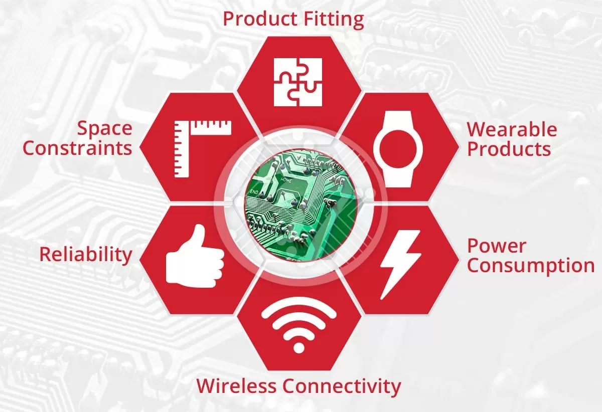
For example, AI can be embedded in the precision placement tool, which can help determine how each component should be placed so as to improve performance. This can also significantly reduce the time required for assembly, which further impacts cost. The use of AI is also known to reduce the bill of materials or BOMs. Essentially then human designers can be augmented with state-of-the-art artificial intelligence to design your board faster as well as at a lower cost.
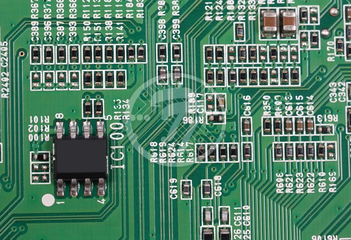
Another advantage with using AI is that it can quickly do an inspection based on the common location for a defect and narrow down defects with ease and in a manner that saves time. Also with real-time problem-solving, manufacturers can potentially save millions of dollars in repairs as well as lost businesses.
Requirements for successful implementation of AI in PCB manufacturing industry
Successful AI implementation in Smart PCB manufacturing, however, requires deep expertise in both verticals- PCB manufacturing as well as AI. What is needed is that process expertise is supported by operational know-how. Also AI can be successful when high quality data is put to use. Defect classification, for example, is an important aspect of having an automated solution that provides optical inspection. With an AOI machine, images of defective PCBs can be sent to a multi image verification station, which may be in a remote location. The defects may then be classified as true or false defects. The same thing when done with human intervention is not only expensive but also prone to errors. The AI system on the other hand provides accuracy provided of course accurate data is available. Small changes in data can of course lead to a host of changes and hence data sensitivity is of utmost essence.
The other aspect besides accuracy of data that ensures success of AI in PCB Manufacturing is a strong collaboration between the AI solution provider and the PCB manufacturer. It is important that the AI provider has enough understanding of the PCB manufacturing process to be able to create a meaningful system. It is also important that the AI provider invests in R&D so that it can offer up-to-date robust solutions that are effective and efficient. With effective use of AI, the provider will help the business in more than the following ways:
- Help recast business models as well as business processes- With intelligent automation, process will be optimized
- Unlock the trapped value of data- AI can be used to study data analytics as well as to discover trends and generate insights
- Change the relationship between humans and machines- With the use of AI, the manpower will be able to spend more time on non-routinized tasks.
Going forward, AI will result in improved processes as well as exponential speed which will in turn go a long way in taking the PCB manufacturing industry to a whole new level. It is only a matter of time where Industrial companies also become digital companies with customers becoming totally centric to their operations. As AI becomes more and more mainstream within organizations, it will see improved trust and dependability and will become mission critical to organizational success.
Technotronix offer Electronics Manufacturing Service with combining state-of-the-art technology and advanced engineering to deliver unparalleled quality and service. Our prolonged goal is to serve our customers with electronic telecom solutions for development in telecommunication industry and to create advanced IT applications for our customers globally. To acquaint with Technotronix, reach us at sales@technotronix.us to get more information for PCB Manufacturing services for electrical telecom applications or prototypes!