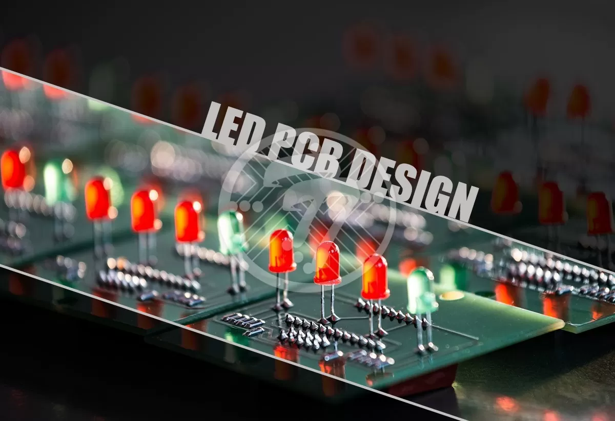
LED PCB design guide – What are the design considerations?

By | Date posted: | Last updated: December 11, 2025
LED PCB design

The use of LED PCBs must quite an extent become ubiquitous with many applications making use of them. In fact, the use of LEDs in standard printed circuit boards is quite a technological revolution. They offer several advantages including but not limited to:

  • Low Cost.
  • High on efficiency in terms of power consumption.
  • Compact structure including their light weight and small size.
  • Resistance to dust & moisture.
  • Improved lifespan, and more.

To avail of the many advantages offered by LED printed circuit boards, however, it is imperative that some key design aspects be kept in mind. Here is a quick look at some of them.

Key considerations in LED PCB design

Component placement

One thing that is crucial when it comes to LED PCB design, it is proper component placement. With the right component placement you can not only ensure easy manufacturability but also ensure quality.

It is important to maintain a certain distance when it comes to placement of components on the board else it can lead to overvoltage. It is therefore important to consider two aspects:

  • Creepage or the shortest distance between components.
  • Clearance or the distance between components measured through the air.

It is also important to ensure that the components are not placed near the PCB outline. Placing components towards the edge can lead to dislodging of components.

Also, it must be kept in mind that all Surface Mounted components follow the SMD PCB design rules. Through-hole components similarly must be placed on top of the board so that the number of steps required for assembly, are optimized.

As for blind and buried PCB vias they should not be placed too close to SMT pads as doing that can mean that the solder can migrate away from the pad. In such situations, there is the possibility of a faulty joint. As a thumb rule, therefore, a distance of 0.025 inches or more should be maintained between the vias and the SMT pad.

PCB materials

While considering the PCB design, it is also important to take into account the material used. The two popular choices include FR4 and IMS or what is known as Insulated Metal Substrate. In choosing the PCB material you need to be mindful of the fact that it not only ensures that excess heat is removed from the board but it also provides electric insulation.

When it comes to the metal base layer, aluminum is a popular choice as it ensures thermal management.

Thermal management

High temperature can impact the longevity of LED lights. To ensure thermal management, therefore, the following are used to dissipate heat:

  • Aluminum Cores
  • Thermal Vias
  • Heat Sinks

For thermal management it is also important that the right component placement be undertaken.

Tracking

Careful tracking is a prerequisite in order to ensure there are no short circuits or crosstalk. If there is proper trace routing, you can rest assured that there is no interference from other networks. The right track width also goes a long way in preventing overheating. It is also important to pay due attention to:

  • Tracking Space
  • Mounting Holes

Finishes

The finish of the board helps in protecting the copper as also offering a soldering surface. Some of the common finishes include:

  • HASL
  • OSP
  • Electrolytic Nickel
  • Electrolytic Gold
  • Immersion Tin
  • Immersion Silver, and more.

The pros and cons of each finish need to be carefully ascertained.

To Sum Up

When it comes to LED PCB, we need to ensure that the following challenges are suitably mitigated:

Heat – The design should ensure that there is optimal thermal management so that longevity is maintained. This is because the temperature of the LED circuit has an inverse correlation with the longevity of the LED.

Color of the light – Once the temperature of the LED circuit increases the colors of the LED can change. Therefore proper heat dispersal is key.

Efficient PCB design, therefore, is a key aspect of manufacturing the right LED solution. It is imperative that you choose the right partner who has the requisite industry knowledge and can also ensure that the PCB designs are customized to the bespoke needs of your applications.

At Technotronix, we are fully equipped to handle your LED PCB manufacturing requirements. With over four decades of experience in delivering high-quality, on-time, competitive price products, you can bank on us for your PCB requirements. In case you have any questions regarding LED circuit boards, please feel free to contact us via email at [email protected] or call us at 714/630-9200.

A comprehensive guide to improve automotive PCB design!

By | Date posted: | Last updated: March 18, 2026
Automotive PCB Design

Printed Circuit Boards are an integral part of almost every automobile. In fact the use of sophisticated PCBs has led to the incorporation of revolutionary features in automobiles including but not limited to keyless start, automated parking, autopilot & more.

The board design & layout has a crucial part to play when it comes to improved performance. Here are some deign guidelines to follow that can go a long way in improving efficiency.

Automotive PCB Design Guidelines:

1. Component Placement

Both the placement as well as orientation of components have a big role to play when it comes to the performance of the board. Some thumb rules to follow, include:

  • Ensuring that similar components are placed in the same direction.
  • If you are undertaking wave soldering, the components should be parallel to the direction of the wave.
  • Ensure that inductors come with spaces in between.
  • Inductors should be kept at right angles to each other to prevent crosstalk.
  • The analog & digital components must be separated.
  • Ensure that tall & short components aren’t placed adjacent to each other.
  • High power components should be placed away from other components in order to ensure proper dissipation of heat.

2. Proper placement of leads

  • Leads should not be placed too close to each other.
  • Ensure proper grounding under the leads.

3. Signal Routing

For layers that conduct high current, the use of 2-4 vias is prudent. To ensure proper signal routing, the following principles come in handy:

  • Power and ground planes must be placed on inner layers.
  • Sensitive signals must be protected from noise sources.
  • Use of shortest tracks is advisable.
  • In routing the traces, the direction should be horizontal on one side and vertical on the other.
  • In fact, the vertical & horizontal layers must be placed alternately.

4. Thermal Management

It is imperative that thermal management techniques be employed such that heat is effectively disseminated. Some of the ways to do it include:

  • The use of copper planes & signal vias helps improve thermal conductivity.
  • In terms of placement, the signal vias must be placed closer to the components with surface pins.
  • Where there are high-power components, it is important that heat sinks be placed.
  • The use of metal thermal pads is also prudent.
  • Solid-filled vias also help transfer heat effectively.
  • Using metal core for the board is yet another effective strategy.
  • The use of high Tg boards is also recommended.

5. Design Rules

Some of the design rules to follow as practice include:

  • Ensure that there is appropriate spacing between components.
  • Similarly, the spacing between the power supply & ground wires needs to be adequate.
  • Ensure that the PCB layout connectivity is in sync with the schematic.
  • The outer rim of the power layer should be reduced in order to avoid short circuits.
  • Ensure that you verify the signal integrity, power integrity as well as electromagnetic interference.
  • Check to see that the ground connections are adequate.

To sum up

No marks for guessing that automotive designs will continue to get more and more complex. In fact with advanced driverless cars, the complexity will only go up. It is therefore extremely important that automotive design adheres to the following standards:

  • IATF 16949
  • IPC- 6012 Class 3
  • AEC-Q100

In fact, IPC-6012 offers a number of guidelines for automotive PCB design. Some of these specifications include:

  • The position accuracy of holes allows for a tolerance of 100 microns.
  • There needs to be a minimum drill hole size.
  • The hole wall separation needs to be no more than 40% of the dielectric thickness.
  • Ensure that there si no contamination before application of the solder mask.
  • Post the soldering process, preconditioning needs to be undertaken to look for cracks, open & short circuits.
  • Solder Mask parameters need to adhere to IPC- 6012DA.

In addition, if Class 3 boards are being manufactured to cater to crucial applications, the following points will come in handy:

  • The PTH should be 15 mils over the diameter of the lead.
  • The internal annular ring should not be less than 1 mil while the external. annular ring should not be less than 2 mil.
  • Pattern tolerances need to be adhered to.

Adherence to the above pointers will ensure that the PCB design for automotives can cater to the most complex applications.

Technotronix is a skilled and experienced professional in providing secured automotive electronics and PCB manufacturing service. We have state-of-the-art equipment and an experienced team that can deliver quality PCB assembly and prototypes that do justice to the ever growing and dynamic demands of automotive industry.

What is PCB cloning? How does it work, and what are its advantages?

By | Date posted: | Last updated: December 11, 2025
PCB Cloning

Also referred to as PCB duplication, PCB cloning is a reverse engineering technology that is applied in order to create copies of existing PCBs. It ensures that you can create the exact design of the PCB without going through the laborious design process. It therefore is extremely effective when it comes to saving time as well as cost.

With electronic gadgets evolving continuously, it is hard to use traditional R&D methods to keep pace. Reverse engineering is therefore a powerful option. Not only does PCB cloning extend the life of a device when components become obsolete, it also helps you modify existing designs to meet your bespoke requirements.

How does PCB cloning work?

Done by way of a simple, automated process, the starting point for PCB cloning is for you to have the detailed bill of materials (BOM) as well as the circuit schematics. The steps involved in the cloning process are as under:

  • Ensure all active components are removed from the PAD hole & the tin. An ultrasonic is next used to clean the board. The empty board is now scanned.
  • Launch Photoshop & copy the scanner to the program.
  • A paper yarn can be used to polish the board. The board is next kept on the scanner & Photoshop is re-launched.
  • Next the picture is saved as a BMP file.
  • Convert the BMP file into PROTEL. Open PROTEL99 & create a PCB file. CAD needs to be imported next and the file saved. 2 levels are to be generated with the PROTEL file.
  • Open the CAD files. Next copy the component package into the CAD using the PCB image as reference. Next ensure that the pads & vias are placed correctly. Arrange the pads as per their sizes.
  • Next a line needs to be drawn on the top layer & the devise needs to be installed. This needs to be followed by deleting the silkscreen layer.
  • Convert the PCB to PROTEL & integrate the diagrams.
  • The next step involves printing the layers on a film and putting the film on the PCB.
  • Test the cloned PCB.

Advantages of PCB cloning

PCB cloning offers a wide variety of benefits. Some of these include:

Optimizes time and cost

While normally PCB manufacturing is time-consuming as well as costly, PCB cloning helps you in both these aspects. Besides not having to work on the design, it also ensures that you save on PCB testing as well as the creation of PCB prototypes since the original design is well-established.

Simplifies production

It makes the production process simple as manufacturers can reverse engineer innovative designs. With the automated process the entire production process is streamlined. It also helps automate manufacturing processes & saves time & money that come with manual labor. It also ensures production of high-performance & long-lasting boards.

Improved scalability and freedom

It offers flexibility to companies to be adaptable throughout the manufacturing process and to create boards that meet the needs of the consumers. Also, it lends itself to scalability as a large number of boards can be produced from a single PCB design.

Building Customer Friendly Products

With cloning of PCBs engineers build customer-friendly products by reverse engineering the current impactful PCB designs.

Offers Production Flexibility

With PCB Cloning you can use a single design to mass manufacture products.

Consistency in performance

The cloned boards offer consistency in performance since the design has already been tried & tested.

Improves timelines

In a milieu where competitive advantage is derived from quick time-to-market, PCB cloning brings a major benefit. The process is now not only simple but extremely short too.

To sum up

To sum up, PCB cloning ensures that the process is easier, its cost is lower & that PCB production capacity is enhanced. It is no surprise then that manufacturers prefer cloning as opposed to constructing a PCB schematic from scratch.

The one thing to keep in mind though when it comes to PCB Cloning is the issue of copyright as it protects the interest of the original designer.

Technotronix provides a one-stop solution for PCB manufacturing services with specialized support, reliable testing, and multi-functional features. In case if you have any questions, please feel free to contact us via email at [email protected] or call us at 714/630-9200.

Best practices for avoiding solder balls to ensure flawless SMT manufacturing!

By | Date posted: | Last updated: December 11, 2025
SMT manufacturing

A big issue when it comes to Surface Mount Technology (SMT) manufacturing is the formation of solder balls. These can be caused on account of a wide variety of reasons and can result in several issues even causing the end product to fail. Let us look at what exactly solder balls are and importantly what are the ways to avoid their formation.

What are Solder Balls?

Essentially these are balls of metal alloy that are formed on the surface of the PCB once the soldering process is completed. The formation of solder balls, impact the functionality of the PCB. They can even impact the quality of the component joints especially if they are large in size. Even more damaging is the fact that if these solder balls roll onto other board parts they can cause shorts.

Some of the reasons that lead to the formation of solder balls include:

  • High humidity
  • Excessive flux in the solder paste
  • High temperature or pressure during the reflow process
  • Improper cleaning post flow

Top ways to prevent solder balls

Some of the ways to avoid formation of solder balls include:

1. Ensure there isn’t too much moisture

You need to take care that the board is free of moisture. For this, it is important to store the PCB in a dry place. Also it is important to dry the board before production with anti-static cloth. Also, baking the boards at 120 degree Celsius works for four hours works well to ensure that excess moisture evaporates.

2. Choose the right solder paste

Solder paste that is high on metal content has fewer chances for solder balls to form. It is also important to ensure that there isn’t too much flux in the solder paste. While Flux can be used to prevent oxidation however excess of it can lead to a structural collapse.

3. Preheat the PCB

It is important to preheat the boards so that they are as close as possible to the oven’s temperature. This will ensure that the solder melts evenly.

4. Ensure that the solder mask is in place

Ensure that the solder mask is in place and that the solder paste is used properly so that there are no gaps between the traces & the pads. Using high quality equipment as also keeping the rate at which the board is preheated, low are other ways to ensure that the solder spreads evenly.

5. Ensure that PCB mounting stress is under control

If there is a lot of stress on the board when it is mounted, the traces & pads can stretch or condense. If there is too much inward pressure the pads will be pushed closed. On the other hand, if the pressure is too much outwards the pads will be pushed open.

6. Ensure pad spacing is correct

Incorrect pad spacing can lead to issues in solder pooling. Incorrectly placed pads can, not only cause solder balls to form but also for them to fall out & cause shorts. The pads must therefore be placed optimally.

7. Ensure that the stencil is clean

It is important that the excess solder paste is cleaned off the stencil. Any excesses can lead to formation of beads or balls. In fact after each round the stencil should be cleaned. While this may involve time, it will ensure that it does not lead to costly errors.

8. Ensure that the stencil dimensions are correct

It is important to choose a SMT stencil with the right thickness. Stencils that are too thick do not work well. Additionally, stencil opening ratios & shapes need to be paid due attention to.

To sum up

Solder Balls can lead to a wide variety of issues. However, fortunately with some basic precautions you can prevent their formation. It is imperative that you look at your production process step-by-step & ensure that you take the necessary steps so that the formation of solder balls can be prevented. With the above tips you can ensure that the risk of solder ball formation is minimized. It is important that you choose the right electronics contract manufacturer who has the requisite experience and stringent quality control measures to offer high quality PCBs.

At Technotronix, we are fully equipped to handle your PCB manufacturing requirements. We have over 40 years of experience in SMT PCB assembly. Our team of experts and state-of-the-art manufacturing facilities ensure that all our PCBs meet industrial standards. If you are looking for high-quality SMT PCB solutions, you can submit your requirements via PCB SMT assembly quote form. Also, if you have any questions, please feel free to contact us via email at [email protected]