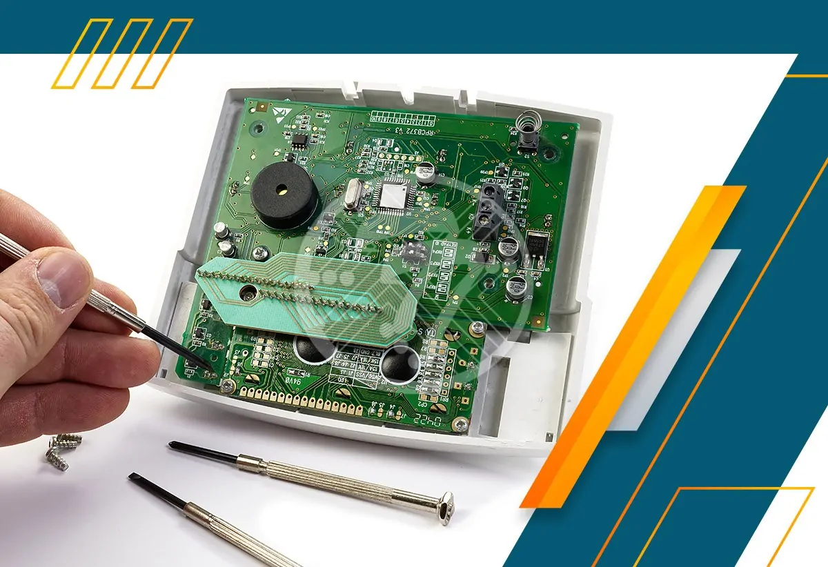
PCB AOI: Role of Automated optical inspection in PCB Manufacturing

By | Date posted: | Last updated: December 11, 2025
PCB AOI

The importance of testing in PCB manufacturing cannot be overstated. With PCBs being used for mission critical operations, the integrity & smooth functioning of the PCB is central to the efficacy of the device.

One of the important tests to check whether the PCB has any manufacturing faults is Automated Optical Inspection or what is popularly known as AOI.

What is Automated Optical Inspection (AOI)?

Essentially as its name suggests, it is a machine-based technique that checks the PCB for any potential defects such as:

  • Surface Defects
  • Dimensional Defects
  • Component Placement Defects

With complex circuit boards and boards being manufactured in large quantities, manual checking becomes more & more difficult. AOI therefore has emerged as an important tool to check efficacy of the board at cost effective price points. Let us look at how it really works.

How exactly does AOI work?

Essentially the process works as follows. A first article PCB is manually inspected. Found good, it is established as a “golden” unit. The AOI then learns from this unit what the gold standard is, in terms of various aspects such as component placement, solder joints and more. This information is then stored in its database. The AOI system then compares each new board with this unit & alerts the operators in case of any inconsistency. The AOI system is equipped with high-resolution cameras, which capture a wide array of images, which come in handy for the comparisons. Different equipment works well for different kinds of inspection. So, while solder paste inspection is done by way of laser scanning, an assembly verification system relies on imaging.

Some of the methods that AOI makes use of, include:

Template matching – Simply put, this is a pixel-by-pixel method, where a small template is applied to a large inspection image. Normalized Cross Correlation is then calculated between the template & inspection image.

Object recognition – This method simply relies on a comparison between the ideal image & the captured image

Blob analysis – This involves separating the object from the background & then generating a blob by grouping object pixels.

Advantages of Automated Optical Inspection

AOI offers a wide range of advantages including but not limited to:

Miniaturization

With the increasing trend of miniaturization, the size of PCB components is constantly on the decline and component density is high. In such a scenario, AOI comes in extremely handy in checking for the positional accuracy of components. The advantage with AOI is that it can detect even small deviations in position eliminating chances of a defect.

Versatility

The big advantage with AOI is that it is useful not only in case of PCB fabrication but also in PCB assembly where it helps in checking for aspects such as soldering and polarity. The fact that AOI can be used at any stage makes it an ever so important tool when it comes to inspection efficacy

Programmable lighting

AOI makes it possible to configure light arrays within the inspection software. In turn, this is an invaluable tool that helps in a wide range of defect detection.

Data collection & Retrieval

AOI also helps in collection & retrieval of data which can take different formats such as image, data, text & more.

Cost Advantage

That AOI can help detect any manufacturing defects & save you from costly errors at a later date, makes it an extremely cost-effective process.

Let us also look at some of the defects that AOI can help check. These are on the spectrum of both Fabrication & Assembly.

Fabrication:

  • Shorts
  • Any violations in trace width
  • Spacing violations
  • Excess copper
  • Missing component footprint pads.
  • Drilled hole breakouts in PCB pads

Assembly:

  • Inspection of solder paste.
  • Finished solder joints.
  • Checking the alignment of components
  • Polarity indicators for component orientation.
  • Marking of components
  • Location of fiducials.
  • Labels as well as other markings.

With the ability to capture a wide range of defects, little surprise then that AOI finds wide application. What it offers is both quick & accurate inspection of errors and thereby it ensures high quality PCBs. Right from bare circuit boards to the SMT Assembly line, its importance is therefore ubiquitous.

Technotronix is one of the leading PCB manufacturers in the USA, providing custom, lead-free and RoHS compliant PCB manufacturing solutions. Whether your requirement is for prototypes or large production runs, we have you covered.

Email us on [email protected] or call us on 714/630-9200 to solve your queries related to our standard PCB services.

All about circuit board schematics that you should know!

By | Date posted: | Last updated: December 11, 2025
Circuit Board Schematics

If putting together a functional circuit board was likened to putting together a tasty dish, the circuit board schematics would have to be the recipe that makes all the difference.

What really are circuit board schematics and how do they work?

With the increasing trend towards miniaturization, an electronic circuit board can be quite complex. Essentially a schematic diagram gives you information about which components are used & importantly how they are connected to each other.

With a dense topology, PCB diagrams become increasingly important. In fact the importance of a PCB diagram can be adjudged if one was to look at the sheer number of processes that are involved in making a circuit board.

The PCB fabrication process itself consists of sub processes such as imaging, etching of layers, arranging the layers, drilling holes, plating vias, applying solder mask, silk screen and more. This is followed by the printed circuit board assembly process, which comprises of picking & placing components, soldering, cleaning, and more.

A circuit board schematic makes the circuit easier to understand and helps tremendously in board development and production.

Difference between PCB Schematics & PCB Design

Often times the terms PCB schematics as well as PCB Design are used interchangeably. The fact remains that they aren’t the same. While a PCB schematic is a two-dimensional circuit design that shows connectivity between PCB components, a PCB design, is a three dimensional layout. The PCB schematic plays an important role in the PCB design. While a schematic lays down how the PCB will finally achieve the desired connectivity, the design becomes the physical representation of the schematic and shows location of components as well as their connections. It is the PCB design that allows engineers to build the PCB.

Building Blocks for a Circuit Board Schematics

Here are some of the building blocks of a schematic:

Cover Page – As its name suggests, it gives an idea of the contents of the schematic. Simply put, it enables you to understand the scope of the product.

Project Statement -This delineates the purpose of the project, its goals & targets. Essentially it offers a high level understanding of the project which makes understanding the rest of the schematic, simpler.

System Block Diagram – This explains the features, functions & the modules that are required to make the product.

Component Schematics of every block – These are circuit diagrams of each functional block. On this basis the costs of the components and the board prices can be determined.

Standard Consistent Reference Designators – The Alpha-Numeric reference designators give an idea of the devices placed. These help us interpret the schematic easily.

Mechanical Components – Essentially these offer details of the devices that may not be a part of the board but which are needed for the final product.

Parts Library – Ensuring that the parts information is critical so that there is minimum rework at a later time. This will also ensure that creation of the BOM is smooth.

Revision Notes – A good set of notes will ensure that there is no confusion in the case of revisions.

Title Block – A title block with the name of the project, the designer, date it was created comes in handy in quick identification.

Below are some important aspects to follow when it comes to the circuitry, to ensure that the circuit board is readable & usable for different stakeholders.

Logic Flow

It is important that logic & connectivity is consistent especially when it comes to high-speed circuitry. It is the basis of the logic flow of the schematic that signal paths will be put together.

Legibility

While this may seem obvious, the fact remains that in a dense schematic with a lot of symbols, nets & pin numbers, you need to ensure that everything is legible. In its absence there can be guesswork, which comes at its own price. It is important to ensure that the reference designators, part numbers & more are not covered.

Creating Net & Component Classes

Creating different net & component classes will ensure that you take into account the design constraints specific to these classes.

Properties

The use of a property editor can ensure that you can adjust the properties in the schematic, such as the values of a selected part & more.

Text Information

It is imperative that the schematic contains text information such as:

  • Part Numbers
  • Product information
  • Company contact, and more

Design Rule Checks

The importance of this aspect cannot be over emphasized. It is absolutely imperative to run a Design Rule Check in a schematic. This will ensure that there aren’t costly errors to contend with at a later date.

Simulation and PCB Layout

While following the points above, you will ensure that you make sure that your circuit board doesn’t have any connectivity errors, but you still need to make sure that the circuits perform well. You can make sure that this happens by running the schematic through a simulator. Any unexpected behavioral issues will show up in this process. Needless to say, that it ensures that you do not have to spend time & money designing several breadboards.

A final design check & you are ready to transfer the circuit board schematic into the PCB layout.

Technotronix provides a one-stop solution for PCB manufacturing services. With over four decades of experience in delivering high-quality, on-time, competitive price products, you can bank on us for your PCB requirements. In case if you have any questions, please feel free to contact us via email at [email protected] or call us at 714/630-9200.

PCB panel design guidelines for trouble-free product manufacturing!

By | Date posted: | Last updated: December 11, 2025
PCB panel design

The design of a panel plays an important role in ensuring error free production of PCBs. Each panel comprises of several PCBs that are arranged optimally. With panelization, in turn, you tend to reap a few benefits including but not limited to time saving and cost-effective production, standardization and more. Additionally, the panel provides protection to each individual circuit board. Also, panelization improves efficiency as opposed to manufacturing one circuit board at a time since a few circuit boards can undergo all the processing steps together. It is possible to have a homogenous assembly where the panel has a single type of circuit board. On the other hand, it is also possible to have a heterogenous composition where the panel has different types of standard circuit boards in a certain ratio.

There are, however, some important guidelines that need to be followed when it comes to successful and economical design of the PCB panel.

PCB Panel Design Guidelines

Size of the Panel

Typically panel sizes that are less than 2 inches face an issue when it comes to certain machines such as pick-and place or even AOI. The size of the panel therefore needs to be kept in mind. To address this issue you may need to arrange additional PCBs on the panel or even add some free area around the edges. It is worthwhile to remember that there are also some maximum dimensions to be kept in mind. Typically the maximum dimension is 12″ x 18″ (305 mm x 460 mm).

Form of Panel

If the PCBs have irregular contours, you will be required to add a handling edge around them. This is necessary since machines such milling machines & saws can handle fixed geometric shapes.

Margin for Panel handling

In transporting the panels, it is important that a narrow strip be left free around the edges. For single sided or double-sided structures, the width of the edge can be 12.5 mm while for multilayer boards it can be 25 mm.

Distance between PCBs

It is the separation method that is used that determines the distance that you need to maintain between individual circuit boards. For example, while in case of laser depaneling the distance can be a few hundred µm, for milling, however, it needs to be 2-3 mm.

Distance between cutting edge and components

The distance of the cutting edge from the mounted components is key. Typically the higher the components, more the distance that needs to be maintained. The distance is also dependent on the cutting method & tools used. If you are using a laser beam you can have components at a distance of 100 µm.

Cutting process

The panel also needs to be prepared according to the cutting process being followed. One of the methods is breakout-tabs. If the panel is prepared in advance you can increase the speed as well as the throughput time. Similarly you can also follow the V-Groove method. In this method the panel is cut from above & below removing 1/3 of the material from each side. This method though may not work best for overhanging components.

The other method of separation which does not involve V-Grooves or tabs is laser depaneling. The laser beam requires a cutting channel that is 200 µm wide as opposed to a milling machine where the requirement is between 2000 and 3000 µm. On account of the saving, you can have more PCBs per panel. Not only do you tend to save on the material, but you also ensure that the processing of the panel is far more effective.

To Sum Up

When it comes to the design of the panel, the above factors play a critical role. In turn, these impact the quality as well as the cost of the PCB. While the design of a PCB panel is complex, taking into account numerous factors, a professional PCB manufacturer is equipped with the necessary experience & expertise as also with industry best practices to ensure that the most optimal design is chosen that has an implication on:

  • The quality of the PCB
  • Its cost
  • Overall profitability of the project.

Technotronix provides a one-stop solution for PCB manufacturing services with specialized support, reliable testing, and multi-functional features. In case if you have any questions, please feel free to contact us via email at [email protected] or call us at 714/630-9200.

Top 10 Best PCB routing practices!

By | Date posted: | Last updated: January 28, 2023

Routing a circuit board comes with its own set of challenges. Especially when we are dealing with miniaturized boards and high-speed signals, the challenges get further enhanced. If you are looking for industry best practices when it comes to PCB routing for high-speed designs, here are 10 handy tips:

PCB routing practices

1. Have a common ground plane below signal traces

It is recommended that high-speed signals be routed over a solid ground plane. Using at least a 4-layer PCB is also beneficial, as then one of the layers can be used as a ground plane. While sometimes a double-sided PCB may be required to be used, the fact remains that when you need to route tracks on both sides, you do not get a solid ground plane. In such cases, at least under critical sections, a ground plane should be attempted. Broadly, full single ground planes offer better results than split grounds.

2. Ensure vias are placed in a grid

It is imperative that blind and buried vias are positioned accurately as otherwise it can result in hotspots. As a thumb rule, vias should be placed 15 mils apart from each other.

3. Ensure that trace bends are kept at the minimum

When routing high-speed signals, bends need to be kept at a minimum. In the situation where you need to keep the bends, 135 degrees is a far better option than 90 degrees. This will ensure that PCB etching is smooth.

4. Maintain a minimum distance between traces

This will ensure that there is minimal crosstalk as among other things, crosstalk is a factor of the distance between traces. Due emphasis therefore needs to be placed on the fact that the traces aren’t closer than desirable.

5. Daisy Chain Routing

If long stub traces are used, there is often a compliance issue with EMC standards. Besides this, signal integrity can be negatively affected. In case it is important to use pull-up or pull-down resistors, it is recommended to use daisy chain routing.

6. Avoid placing components between differential pairs

It is important to have differential pairs parallel to each other. Also, symmetrical routing should be followed for differential pairs. Placing of vias or components between the differential pairs is a strict no-no as it could lead to issues with impedance. In case you need to include serial coupling capacitors, ensure that they are placed symmetrically. Another aspect to keep into account is that both traces should be routed on the same layer.

7. Avoid a split plane while routing signals

The use of a split plane needs to be avoided as such a signal path can lead to EMI issues. If you have a situation where the plane is split between a sink & source, the signal trace is best routed around it. Similarly, if a signal needs to be routed over two different reference planes, stitching capacitors should be used. The position of the capacitor is crucial as the distance between the forward & return path needs to be kept small.

8. Ensure that the analog & digital ground planes are kept separate

This will make it easy to determine which components should be connected to the digital ground & which one to the analog ground. For mixed signal circuits, the analog & digital ground needs to be connected at a point. Zero-Ohm resistors between analog & digital sections are recommended. Also, if the mixed signal design has split planes, you need to take care to see that the digital signal is not routed over an analog ground plane & vice versa.

9. Create a virtual separation in the layout with respect to analog & digital ground

This virtual separation needs to be kept in mind during the routing process. Due care needs to be maintained to see that the analog or digital trace does not crossover to the other side.

10. Keep the width of the component as close as possible to the track width

By doing this, the impedance matching issues between the track & the component pad can be addressed.

With the above tips, you can ensure that your design is robust & that there are no manufacturability issues, causing you loss of precious time when the industrial printed circuit board comes to the manufacturing stage.

Technotronix provides a one-stop solution for electronics manufacturing services with specialized support, reliable testing, and multi-functional features. In case if you have any questions, please feel free to contact us via email at [email protected] or call us at 714/630-9200.